Intro
In my last blog post I alluded to the fact that you could take s1p touchstone files generated by nanoVNAsaver and use this to automatically calculate/simulate a matching network in QUCSstudio. This could be used to quickly design antenna matching networks for instance. I was asked in the comments about exactly to do this. Of course, I had totally forgotten!!! But lets go through it again.
A matching network is normally a network of inductor or capacitors selected to convert from one impedance to another. However it is possible to use alternative components such as transformers, transmission lines, or even resistors as part of an matching network. Once you get to grips with the basics here, you can always experiment in QUCSstudio with alternate components.
Step 1 – Measure your DUT
The Device Under Test could really be any device, but as I am an antenna geek, lets assume its an antenna. I won’t go into detail here about how to measure an antenna as this was covered in my previous posts. However I will highlight one critical point. We must be very careful to understand the calibration plane of tour antenna. If we design a matching network it will be assumed that this is where we place our components. As normal the accuracy you need for this is dependent upon the required frequency. Try to think if you error is likely to be a significant fraction of a wavelength.
Once measured you will need to export a ‘touchstone’ s1p file. This is just a human readable csv file that lists the phase/magnitude(or equivalent representation) of the S11 measurement at every frequency.
Step 2 – Create a QUCSstudio schematic
The easiest way to create this is with an s-parameter template as show below.
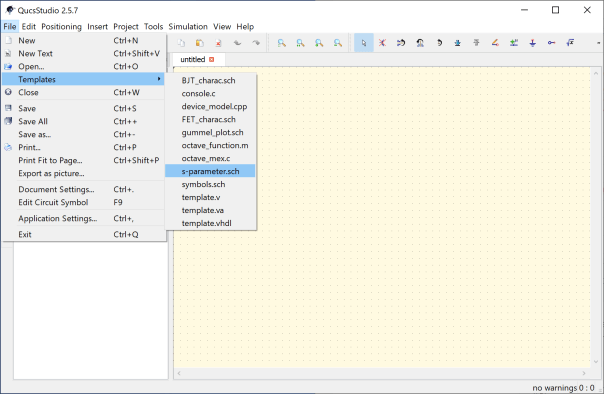
QUCSstudio S-Parameter Template
You should end up with a basic template as shown below.
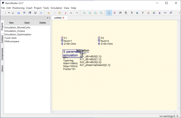
S-Parameter Template
You can test this works by connecting a wire between P1 and P2 and hitting he ‘simulate’ gear icon (or press F2). After a short calculation you should see a Cartesian and Smith chart plot. This wont be ery interesting as we have a perfect 50ohm to 50ohm match.
Perfect match
Import s1p file
To do this we need to remove port 2(P2) and add an ‘S parameter file’ component. Connect it up as shown. You will note the extra unused port on the right hand side of the component. It looks a bit messy on my screenshots due to QUCS not playing nicely with Windows highDPI scaling. We will remove this extra port next.

S-parameter File Component in ‘Systems Components section
If you double click on the component, you will enter the options menu and be able to select your s1p file as well as set the number of ports to 1.
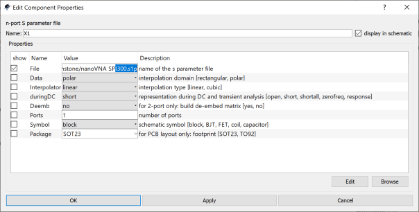
Select you s-param file and set number of ports to 1
We now need to change our simulation parameters to match the frequency range of our touchstone file. This doesn’t need to be exact as QUCS will interpolate between readings. I also needed to change the sweep from log to linear.
We also need to remove references to port 2 in the equations.

Set Simulation Parameters and Equation to match the changes.
Now when we hit run we should see the same plots we saw on the VNA when we initially measure the device. Note, you will have some errors as we are still trying to plot port 2 that we deleted earlier. Just double click on the plot to open it’s options and delete the dB(S[2,2]) plot.
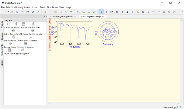
This should look the same as our VNA measurement.
Create a Matching Network
In order to generate this, we first need to add a marker on one of our plots. With this tool selected we can click on our chart to add the marker to a plot. You can fine tune the marker frequency using your arrow keys. I am using the Cartesian plot and choosing 300MHz(3e8) as the frequency I would like my matching network to work at.
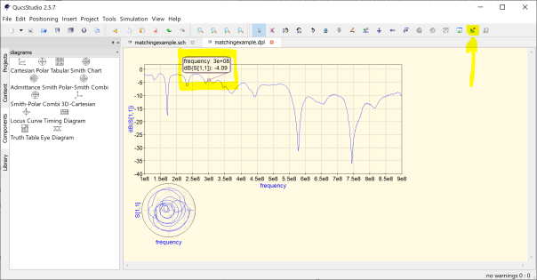
Adding a marker to a plot
To do this we need to right click on the marker until we see the ‘power matching’ option. Clicking this will bring up the Create Matching Circuit dialog box shown below. For mine, I need to change the Import format to mag/deg from real/imag, not sure why.The tool can generate one of 2 solutions depending on if you have ‘use shortest path’ checked. I will simulate both to see how each perform.
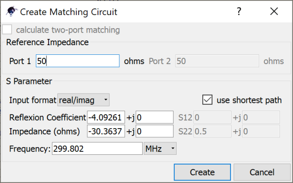
Matching parameters imported from plot
When you click ‘Create’ you will be able to paste a new matching netwrk into your design. This will need to be placed between the Input Port and the S parameter component. The two networks generated in my design are often termed high-pass and low-pass. As can be seen one design has a series L and shunt C and allows for DC current to flow (low pass). The other design is a series C and shunt L, this is a high pass design.
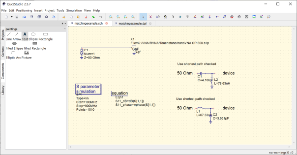
2 matching networks pasted into schematic.
To show the difference, I will simulate both designs as well as the un-matched device.
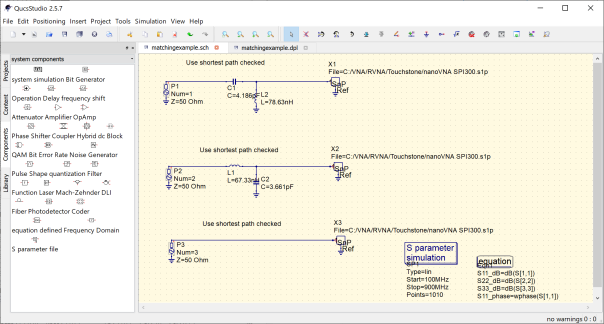
Top to bottom High-Pass, Low-Pass, Unmatched.
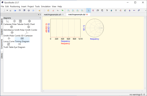
This gives the following results. I will leave it to the reader to work out how to add the extra plots to the chart. It’s not difficult.
For this antenna, we have successfully improved the 300Mz impedance match from about -4dB to -12dB. Although we have made it much worse everywhere else.
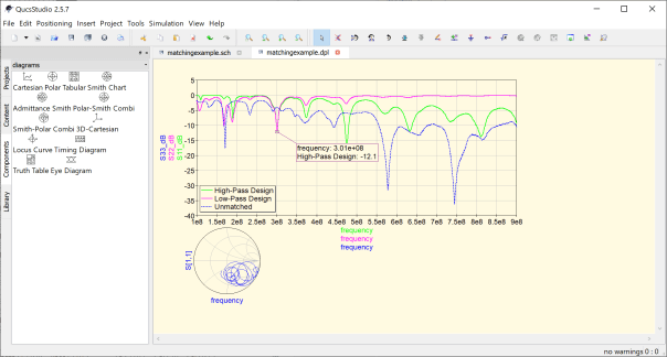
Matching results.
Conclusion
Using both the NanoVNA(or most other VNAs) with QUCSstudio, one can easily import the captured data and design matching networks. QUCS studio allows us to easily predict the performance of these networks. This is just the start however. It is then possible to play with the component values to test out the effect of using real-world values. You can add in additional resistors to simulate real world losses. You can also use the optimisation tools in QUCS sweep parameter values etc.
Note, There is more than one way to skin this cat though. You can achieve similar results using lots of other software such as SimSmithfor example. Software such as Antune can be used with more professional VNA’s to automatically generate more complex matching networks on the fly, using libraries of real world components.
Have fun!!

